- 您现在的位置:买卖IC网 > Sheet目录2005 > LTC2262CUJ-14#TRPBF (Linear Technology)IC ADC 14BIT 150MSPS 40-QFN
11
226214fc
LTC2262-14
For more information www.linear.com/LTC2262-14
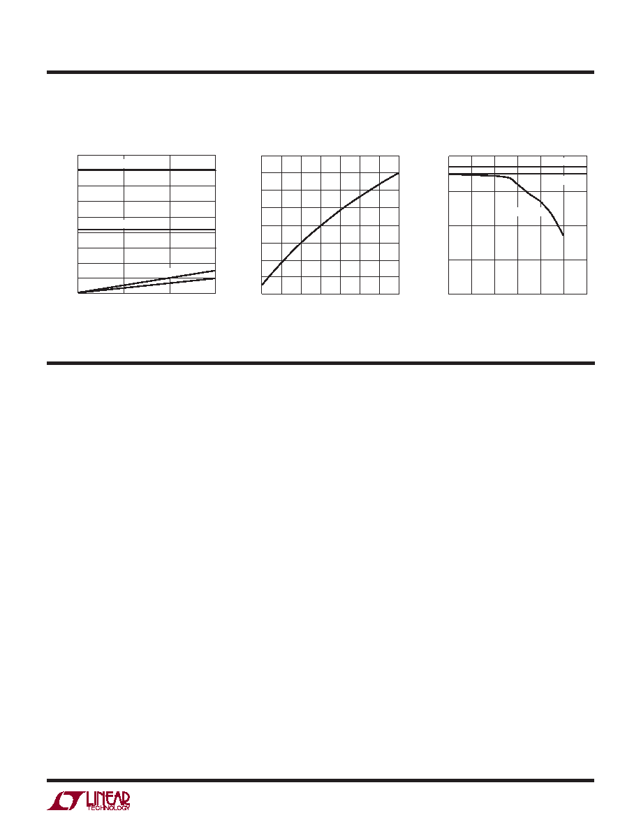
LTC2262-14: IOVDD vs Sample
Rate, 5MHz Sine Wave Input,
–1dB, 5pF on Each Data Output
LTC2262-14: SNR vs SENSE,
fIN = 5MHz, –1dB
TYPICAL PERFORMANCE CHARACTERISTICS
SAMPLE RATE (Msps)
0
25
10
15
20
5
0
45
30
35
40
I OVDD
(mA)
50
100
150
226214 G14
1.75mA LVDS
1.8V CMOS
1.2V CMOS
3.5mA LVDS
SENSE PIN (V)
0.6
71
68
69
70
67
66
72
73
74
SNR
(dBFS)
0.7
0.8
0.9
1.1
1.2
1.3
1
226214 G15
SAMPLE RATE (Msps)
0
69
72
71
70
SNR
(dBFS)
73
25
50
75
150
100
125
226214 G18
DDR CMOS
CMOS
LVDS
LTC2262-14: SNR vs Sample Rate
and Digital Output Mode, 30MHz Sine
Wave Input, –1dB
PIN FUNCTIONS
PINS THAT ARE THE SAME FOR ALL DIGITAL OUTPUT
MODES
AIN+ (Pin 1): Positive Differential Analog Input.
AIN– (Pin 2): Negative Differential Analog Input.
GND (Pin 3): ADC Power Ground.
REFH (Pins 4, 5): ADC High Reference. Bypass to Pins
6, 7 with a 2.2F ceramic capacitor and to ground with a
0.1F ceramic capacitor.
REFL (Pins 6, 7): ADC Low Reference. Bypass to Pins
4, 5 with a 2.2F ceramic capacitor and to ground with a
0.1F ceramic capacitor.
PAR/SER (Pin 8): Programming Mode Selection Pin. Con-
nect to ground to enable the serial programming mode.
CS, SCK, SDI, SDO become a serial interface that control
the A/D operating modes. Connect to VDD to enable the
parallel programming mode where CS, SCK, SDI become
parallel logic inputs that control a reduced set of the A/D
operating modes. PAR/SER should be connected directly
to ground or the VDD of the part and not be driven by a
logic signal.
VDD (Pins 9, 10, 40): 1.8V Analog Power Supply. Bypass
to ground with 0.1F ceramic capacitors. Pins 9 and 10
can share a bypass capacitor.
ENC+ (Pin 11): Encode Input. Conversion starts on the
rising edge.
ENC– (Pin 12): Encode Complement Input. Conversion
starts on the falling edge.
CS (Pin 13): In serial programming mode, (PAR/SER =
0V), CS is the serial interface chip select input. When
CS is low, SCK is enabled for shifting data on SDI into
the mode control registers. In the parallel programming
mode (PAR/SER = VDD), CS controls the clock duty cycle
stabilizer. When CS is low, the clock duty cycle stabilizer is
turned off. When CS is high, the clock duty cycle stabilizer
is turned on. CS can be driven with 1.8V to 3.3V logic.
SCK (Pin 14): In serial programming mode, (PAR/SER =
0V), SCK is the serial interface clock input. In the parallel
programming mode (PAR/SER = VDD), SCK controls the
digital output mode. When SCK is low, the full-rate CMOS
output mode is enabled. When SCK is high, the double
data rate LVDS output mode (with 3.5mA output current)
is enabled. SCK can be driven with 1.8V to 3.3V logic.
发布紧急采购,3分钟左右您将得到回复。
相关PDF资料
LTC2262IUJ-12#PBF
IC ADC 12BIT 150MSPS 40-QFN
LTC2264CUJ-12#PBF
IC ADC 12BIT SER/PAR 40M 40-QFN
LTC2268IUJ-14#TRPBF
IC ADC 14BIT 125MSPS DUAL 40QFN
LTC2280CUP#PBF
IC ADC DUAL 10BIT 105MSPS 64-QFN
LTC2281IUP#PBF
IC ADC 10BIT DUAL 64-QFN
LTC2282CUP#PBF
IC ADC DUAL 12BIT 105MSPS 64-QFN
LTC2284CUP#PBF
IC ADC DUAL 14BIT 105MSPS 64-QFN
LTC2285CUP#PBF
IC ADC DUAL 14BIT 125MSPS 64QFN
相关代理商/技术参数
LTC2262IUJ-12#PBF
功能描述:IC ADC 12BIT 150MSPS 40-QFN RoHS:是 类别:集成电路 (IC) >> 数据采集 - 模数转换器 系列:- 标准包装:1 系列:- 位数:14 采样率(每秒):83k 数据接口:串行,并联 转换器数目:1 功率耗散(最大):95mW 电压电源:双 ± 工作温度:0°C ~ 70°C 安装类型:通孔 封装/外壳:28-DIP(0.600",15.24mm) 供应商设备封装:28-PDIP 包装:管件 输入数目和类型:1 个单端,双极
LTC2262IUJ-12#TRPBF
功能描述:IC ADC 12BIT 150MSPS 40-QFN RoHS:是 类别:集成电路 (IC) >> 数据采集 - 模数转换器 系列:- 标准包装:1 系列:- 位数:14 采样率(每秒):83k 数据接口:串行,并联 转换器数目:1 功率耗散(最大):95mW 电压电源:双 ± 工作温度:0°C ~ 70°C 安装类型:通孔 封装/外壳:28-DIP(0.600",15.24mm) 供应商设备封装:28-PDIP 包装:管件 输入数目和类型:1 个单端,双极
LTC2262IUJ-14#PBF
制造商:Linear Technology 功能描述:ADC Single Pipelined 150Msps 14-bit Parallel/LVDS 40-Pin QFN EP 制造商:Linear Technology 功能描述:IC ADC 14BIT 1.8V 150MSPS 40-QFN
LTC2262IUJ-14#TRPBF
制造商:Linear Technology 功能描述:ADC Single Pipelined 150Msps 14-bit Parallel/LVDS 40-Pin QFN EP T/R 制造商:Linear Technology 功能描述:IC ADC 14BIT 150MSPS 40-QFN
LTC2263-12
制造商:LINER 制造商全称:Linear Technology 功能描述:12-Bit, 65Msps/40Msps/25Msps Low Power Dual ADCs
LTC2263-14
制造商:LINER 制造商全称:Linear Technology 功能描述:Quad 14-Bit, 125Msps ADC with Integrated Drivers
LTC2263CUJ-12#PBF
功能描述:IC ADC 12BIT SER/PAR 25M 40-QFN RoHS:是 类别:集成电路 (IC) >> 数据采集 - 模数转换器 系列:- 标准包装:1 系列:microPOWER™ 位数:8 采样率(每秒):1M 数据接口:串行,SPI? 转换器数目:1 功率耗散(最大):- 电压电源:模拟和数字 工作温度:-40°C ~ 125°C 安装类型:表面贴装 封装/外壳:24-VFQFN 裸露焊盘 供应商设备封装:24-VQFN 裸露焊盘(4x4) 包装:Digi-Reel® 输入数目和类型:8 个单端,单极 产品目录页面:892 (CN2011-ZH PDF) 其它名称:296-25851-6
LTC2263CUJ-12#PBF
制造商:Linear Technology 功能描述:IC ADC 12BIT 25MSPS QFN-40